ARM Architecture's New Frontier: The 2nm Challenge
The engineering hurdles facing the next generation of mobile and server processors as manufacturing approaches physical limits.
By YDT Editorial2 min read
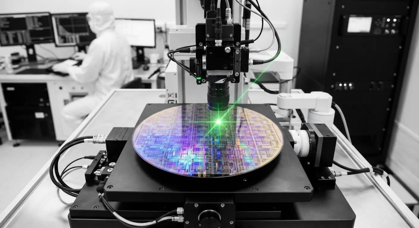
Every process node shrink used to deliver the same bargain: more transistors, less power, lower cost per gate. At 2nm-class geometries, that bargain has broken apart. Density still improves, but power and cost no longer follow automatically — and the architectural consequences are reshaping how ARM-based designs are built.
Gate-all-around changes the design rules
The move from FinFET to gate-all-around (GAA) nanosheet transistors is the defining shift of this generation. Nanosheets restore electrostatic control that fins were losing at short channel lengths, but they arrive with new constraints: fewer discrete drive-strength options, tighter layout dependency effects, and a heavier reliance on design-technology co-optimization between foundry and CPU teams.
For ARM licensees, this means the reference physical implementations matter more than ever. A core that closes timing beautifully on one foundry’s nanosheet process may need a different pipeline balance on another’s. The era of porting a design between fabs with modest effort is effectively over.
Backside power delivery
The most consequential innovation of the 2nm era may not be the transistor at all. Backside power delivery networks move the power rails to the rear of the wafer, freeing the front-side metal stack for signal routing. Early implementations report meaningful IR-drop reduction and routing congestion relief — directly translating into higher sustainable clocks for wide cores.
The cost is manufacturing complexity: wafer thinning, nano-through-silicon vias, and a bonding step that all must yield. Designs that assume backside power cannot be cheaply backported.
What it means for the ecosystem
Expect divergence. Flagship mobile SoCs and hyperscaler server chips will absorb the cost of leading-edge nodes; mid-range parts will linger on refined 4nm-class processes where the economics still work. The interesting engineering will happen in chiplet architectures that mix nodes — putting only the compute tiles on 2nm while I/O and analog stay on mature silicon.
Filed under
Related articles
Hardware29 min read
Oscilloscope vs Logic Analyzer: Key Differences and How to Choose
Oscilloscope vs logic analyzer: how each instrument measures signals, where each one fails, and how to choose the right tool for analog, digital and mixed-signal debugging.
Hardware2 min read
The Future of RISC-V: Decentralizing the Silicon Monopoly
Open-source hardware is gaining real traction in enterprise data centers. A look at the technical hurdles and strategic implications of the RISC-V movement.
Hardware3 min read
Implementing High-Efficiency Power Rails in Next-Gen Microelectronics
Power integrity has become the bottleneck for system reliability. How advanced substrates and smarter regulation are changing power delivery design.
Electronics18 min read
Function Generator vs Arbitrary Waveform Generator: What You Are Buying
Three names, two architectures: how DDS and point-by-point playback differ, what the labels hide, and how to read the architecture off a datasheet.