GaN Transistors: Transforming Power Density
Why gallium nitride is displacing silicon in high-performance power conversion, and where the technology still earns its price premium.
By YDT Editorial2 min read
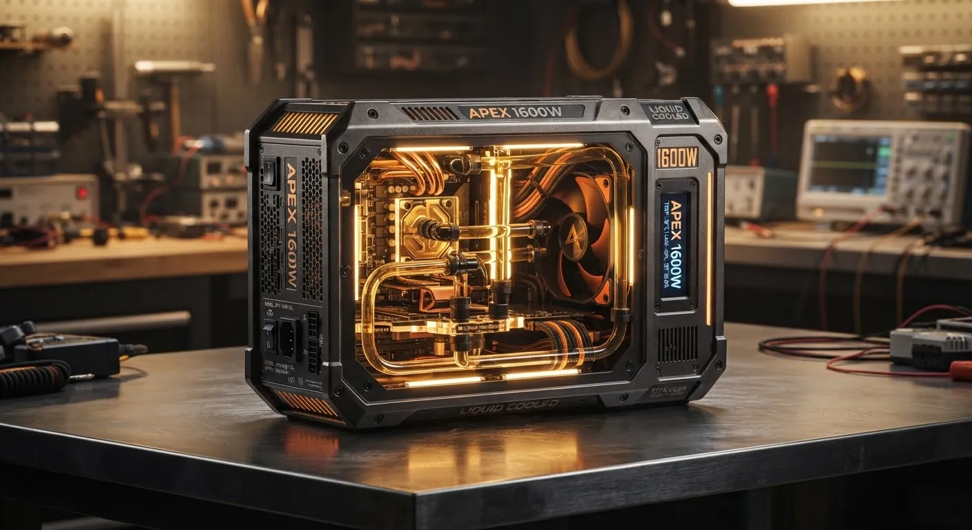
Gallium nitride went from exotic RF material to consumer mainstream in under a decade, and chargers were only the opening act. The properties that made GaN win in fast chargers — high electron mobility, negligible reverse recovery, switching frequencies an order of magnitude above silicon — are now reshaping server power supplies, solar inverters, and motor drives.
The physics of the advantage
A silicon MOSFET switching at 100 kHz spends a meaningful fraction of each cycle in lossy transitions. GaN HEMTs switch cleanly in nanoseconds, which does two things: it slashes switching losses directly, and it allows magnetics — usually the largest and heaviest components in a converter — to shrink dramatically. A 3 kW server supply that needed a brick of ferrite at 90 kHz can hit the same ripple targets with a fraction of the magnetic volume at 1 MHz.
The efficiency story compounds at partial load, where data center supplies actually operate. Titanium-grade efficiency targets that required heroic silicon topologies are now attainable with comparatively simple GaN totem-pole PFC designs.
Where silicon still wins
GaN’s price per amp remains above superjunction silicon, and its avalanche ruggedness — the ability to absorb overvoltage events without dying — is inherently weaker. In applications where cost dominates and switching frequency doesn’t matter (think appliance motor drives), silicon and increasingly silicon carbide keep the socket. SiC in particular owns the high-voltage territory above 900 V, where GaN devices are still maturing.
Design implications
Fast edges are a double-edged sword: dV/dt rates of 100 V/ns turn sloppy layouts into EMI generators. GaN designs demand tight power loops, kelvin-source connections, and gate drives engineered for immunity to ringing. Teams migrating from silicon should budget for a board respin — the first layout that “worked fine with MOSFETs” rarely survives contact with GaN edge rates.
Filed under
Related articles
Electronics18 min read
Function Generator vs Arbitrary Waveform Generator: What You Are Buying
Three names, two architectures: how DDS and point-by-point playback differ, what the labels hide, and how to read the architecture off a datasheet.
Electronics23 min read
How to Choose a Signal Generator: Getting the Signal You Asked For
How to turn a required stimulus into datasheet requirements: the load the instrument assumes, bandwidth against sample rate, reconstruction and vertical resolution.
Electronics22 min read
How to Choose a Multimeter: A Specification-Led Buying Guide
Choose a multimeter by the errors it introduces: burden voltage, input loading, AC bandwidth, safety category and accuracy on the reading you actually take.

Electronics16 min read
How to Use a Thermal Camera: Getting Readings You Can Trust
A thermal camera always shows a number. Learn the checks — emissivity, reflected temperature, focus and spot size — that decide whether it is a measurement.